

Introduction: PCB Manufacturing in the Modern Electronics Era
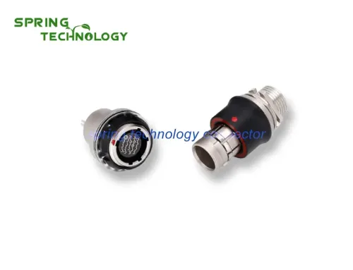
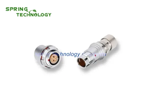
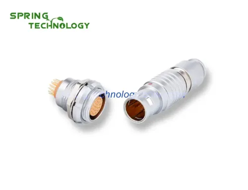
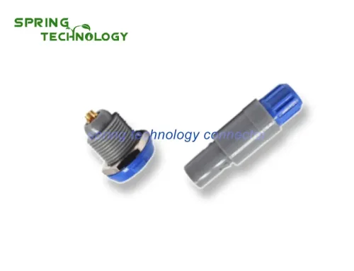
Printed Circuit Board (PCB) manufacturing has evolved significantly since the inception of round push-pull self-locking connectors, which are predominantly used for PCB board installation. As we advance through 2026, the global PCB manufacturing market continues its robust growth trajectory, projected to reach $103.8 billion by 2027 with a CAGR of 4.3% from 2024-2027. This expansion is driven by increasing demand from consumer electronics, automotive electrification, 5G infrastructure, and IoT device proliferation.
Whether you are creating prototypes for connector integration or producing boards for mass manufacturing, understanding PCB fabrication methods remains essential for electronics engineers, hobbyists, and production managers. This comprehensive guide explores traditional DIY techniques alongside modern industrial processes, providing insights into copper-clad board preparation, etching methods, and quality control practices that define successful PCB manufacturing in 2026.
1. Fundamentals of PCB Board Construction
1.1 Copper-Clad Laminate Basics
The foundation of any PCB begins with the copper-clad laminate (CCL), consisting of an insulating substrate bonded with copper foil on one or both sides. Common substrate materials include FR-4 (glass-reinforced epoxy), CEM-1 (cellulose-based), and polyimide for flexible circuits. Copper thickness typically ranges from 0.5 oz/ft2 (17.5 um) to 2 oz/ft2 (70 um), selected based on current-carrying requirements and etching precision needs.
1.2 PCB Layer Configurations
Modern PCBs range from single-sided boards to complex multi-layer constructions with 20+ layers for high-density applications. For connector mounting applications, particularly round push-pull self-locking connectors, 2-4 layer boards provide adequate routing complexity while maintaining cost-effectiveness. Each layer requires precise alignment during lamination, with via structures enabling interlayer electrical connections.
1.3 Design for Manufacturing (DFM) Considerations
Successful PCB manufacturing requires adherence to DFM guidelines: minimum trace width/spacing (typically 0.15-0.2mm for standard processes), annular ring requirements (0.15mm minimum for through-holes), and component placement clearances. For connector footprints, especially precision push-pull connectors, pad dimensions must match manufacturer specifications exactly to ensure reliable solder joints and mechanical retention.
2. DIY PCB Fabrication Method One: Wax Paper Transfer
2.1 Materials and Preparation
This traditional method suits small-batch production and educational purposes. Required materials include: copper-clad board sized to circuit requirements, wax paper, steel plate, fine-tip pen, paint powder (or ferric chloride-resistant ink), soft brush, potassium chlorate, concentrated hydrochloric acid (15%), banana water (solvent), and rosin solution.
2.2 Step-by-Step Process
Step 1: Cut the copper-clad board to dimensions specified in your circuit diagram, ensuring clean edges without copper burrs that could cause etching inconsistencies.
Step 2: Place wax paper on a steel plate and trace the circuit layout at 1:1 scale using a fine-tip pen. Cut the wax paper to match the PCB size, then position it precisely on the copper-clad surface. Prepare printing material by mixing paint powder with binder to achieve thick, consistent viscosity.
Step 3: Using a soft brush, apply the printing material evenly over the wax paper template. Repeat 2-3 times to ensure complete coverage of trace patterns. This wax paper stencil can be reused multiple times, making the method economical for small production runs of 10-50 boards.
Step 4: Prepare etching solution with a ratio of 1g potassium chlorate to 40ml hydrochloric acid (15% concentration). Apply the etchant selectively to exposed copper areas using a brush or cotton swab. The chemical reaction dissolves unprotected copper, leaving only the paint-covered traces intact.
Step 5: Rinse the etched board thoroughly with clean water multiple times to remove all etching residue. Use banana water (amyl acetate) to dissolve and remove the protective paint, then wash again to ensure no corrosive fluid remains. Apply rosin flux solution and allow to dry before drilling component holes.
2.3 Advantages and Limitations
This method offers low cost and minimal equipment requirements, ideal for hobbyists and rapid prototyping. However, trace resolution is limited to approximately 0.5mm minimum width, and consistency depends heavily on operator skill. Not recommended for high-density connector interfaces requiring precise pad geometries.
3. DIY PCB Fabrication Method Two: Pre-Cut Sticker and Tape
3.1 Materials Selection
This technique utilizes pre-manufactured adhesive components available from electronics suppliers. Key materials include: pre-cut pad stickers with various inner/outer diameters (common specifications: D373: OD 2.79mm/ID 0.79mm, D266: OD 2.00mm/ID 0.80mm, D237: OD 3.50mm/ID 1.50mm), adhesive tape in multiple widths (0.3mm, 0.9mm, 1.8mm, 2.3mm, 3.7mm), carbon paper for pattern transfer, and ferric chloride etchant.
Choose paper-based stickers (black color) over plastic-based alternatives (red) for better etchant resistance and adhesion. Tape widths should correspond to trace current requirements: 0.3mm for signal lines, 0.9-1.8mm for power traces, and 2.3mm+ for high-current paths.
3.2 Detailed Application Process
Step 1: Create or obtain a printed board diagram showing pad locations as dots and trace routing as single lines. Accuracy of pad positioning is critical, especially for connector footprints with tight pitch requirements.
Step 2: Cut the copper-clad board to final dimensions and clean the copper surface with fine steel wool or abrasive pad to remove oxidation and ensure optimal sticker adhesion.
Step 3: Transfer the circuit pattern to the copper surface using carbon paper. For simple circuits with experienced operators, this step may be skipped in favor of direct sticker placement.
Step 4: Apply pre-cut pad stickers at component lead locations according to your layout. Then apply adhesive tape along trace paths, selecting tape width based on current requirements. For IC pins with 2.54mm pitch, 0.3mm tape fits between adjacent pins, significantly reducing the need for jumper wires on single-sided boards.
Step 5: Gently tap all stickers and tape with a soft rubber or plastic hammer to ensure complete adhesion to the copper surface. Pay special attention to corners and curved sections where edges might lift. In cold conditions, use a heat gun or hair dryer to warm the surface (40-50C), improving adhesive bonding.
Step 6: Immerse the board in ferric chloride etching solution, maintaining temperature below 40C to prevent adhesive failure. Etching time varies from 30 minutes to several hours depending on solution freshness and copper thickness. Agitate the solution periodically for uniform etching.
Step 7: After etching completes, remove the board and rinse thoroughly. Peel off all stickers and tape, then clean residual adhesive with isopropyl alcohol. Lightly polish the copper traces with fine sandpaper (600+ grit), apply rosin-alcohol solution, and allow to dry. The finished PCB quality approaches commercial standards, with 0.3mm trace spacing achievable between IC pins.
3.3 Practical Applications
This method excels for prototype boards, experimental circuits, and small production quantities (1-20 boards). The author frequently employs this technique for creating test fixtures and proof-of-concept designs requiring connector integration, saving significant time compared to breadboard assemblies while maintaining professional appearance.
4. DIY PCB Fabrication Method Three: Shellac Resist Pen
4.1 Protective Coating Preparation
This technique creates liquid resist ink from shellac (lacquer resin) dissolved in absolute alcohol. Dissolve one part shellac in three parts absolute alcohol, mixing thoroughly until completely dissolved. Add several drops of gentian violet (medical purple dye) to provide visible color for trace inspection. Store the prepared resist in a sealed container (such as an ink bottle) to prevent alcohol evaporation.
4.2 Drawing Techniques and Tools
Begin by cleaning the copper plate with fine sandpaper (800+ grit) to create a smooth, oxide-free surface. Use a duckbill pen (technical drawing pen) or compass-mounted ink pen to draw circuit traces directly on the copper. The duckbill pen features an adjustment screw for controlling stroke width, enabling trace widths from 0.2mm to 1.0mm.
For straight traces, use a triangle ruler or straightedge to guide the pen, producing smooth, uniform lines without edge serrations. The shellac resist dries quickly, forming a hard, etchant-resistant coating. This method also allows freehand writing of component designators, test points, or identification marks in unused board areas.
4.3 Correction and Refinement
If drawn lines spread or bleed, the resist concentration is too low – add more shellac to thicken. If the pen skips or fails to flow, the mixture is too thick – add drops of absolute alcohol to thin. Mistakes are easily corrected: dip a small stick (matchstick) wrapped with cotton in absolute alcohol and gently rub to remove unwanted resist, then redraw the corrected trace.
Once the circuit layout is complete, immerse the board in ferric chloride etching solution. After etching finishes, remove the shellac resist by wiping with a cotton ball soaked in anhydrous alcohol. Allow the board to dry briefly, then apply rosin flux for solderability and corrosion protection.
4.4 Storage and Maintenance
Due to alcohols rapid evaporation, always seal the resist container immediately after use. If the concentration thickens during storage, simply add absolute alcohol and mix until proper consistency is restored. Properly stored resist remains usable for months, making this method cost-effective for ongoing prototyping work.
5. Industrial PCB Manufacturing Processes (2026 Standards)
5.1 Subtractive vs. Additive Methods
Modern industrial PCB fabrication primarily uses subtractive etching (removing unwanted copper from clad laminate) or additive processes (building copper traces on dielectric surfaces). Subtractive methods dominate volume production, while additive techniques gain traction for HDI (High-Density Interconnect) boards with microvias and fine-pitch features below 0.1mm.
5.2 Automated Optical Inspection (AOI)
2026 manufacturing standards require 100% AOI for critical applications, particularly automotive, medical, and aerospace PCBs. AOI systems detect opens, shorts, insufficient annular rings, and trace width violations with accuracy down to 5um. For connector mounting areas, AOI verifies pad geometry and coplanarity to ensure reliable solder joint formation.
5.3 Surface Finishes for Connector Compatibility
Common surface finishes include HASL (Hot Air Solder Leveling), ENIG (Electroless Nickel Immersion Gold), and OSP (Organic Solderability Preservative). ENIG provides flat, oxidation-resistant surfaces ideal for fine-pitch connectors and repeated mating cycles. HASL remains cost-effective for general-purpose boards but may cause coplanarity issues with high-pin-count connectors.
6. 2026 PCB Industry Trends and Innovations
6.1 High-Frequency and High-Speed Materials
5G infrastructure and automotive radar systems drive demand for low-loss PCB materials with controlled dielectric constant (Dk) and dissipation factor (Df). PTFE-based laminates, ceramic-filled hydrocarbons, and modified epoxy systems enable signal integrity at frequencies exceeding 77 GHz for millimeter-wave applications.
6.2 Sustainable Manufacturing Practices
Environmental regulations push PCB manufacturers toward halogen-free laminates, lead-free finishes, and closed-loop etchant recycling. Water-based photoresists and reduced chemical consumption processes minimize environmental impact while maintaining production quality. Circular economy initiatives promote PCB recycling for copper and precious metal recovery.
6.3 Miniaturization and HDI Technologies
Consumer electronics and wearable devices demand increasingly compact PCBs with finer features. Any-layer HDI construction, stacked microvias, and ultra-thin laminates (25-50um core thickness) enable high routing density in minimal board area. Laser direct imaging (LDI) replaces traditional phototooling for sub-50um trace resolution.
Conclusion: Selecting the Right PCB Manufacturing Approach
PCB board manufacturing encompasses a spectrum from hands-on DIY techniques to highly automated industrial processes. For prototyping connector-based designs, traditional methods like wax paper transfer, sticker/tape application, and shellac resist drawing offer accessible, low-cost solutions for small quantities. As production volumes increase or design complexity grows, transitioning to professional PCB fabricators becomes economically advantageous.
Understanding fundamental PCB fabrication principles – copper-clad preparation, etching chemistry, resist application, and quality control – empowers engineers and hobbyists to make informed decisions throughout the product development cycle. Whether creating single proof-of-concept boards or managing thousand-unit production runs, the methods outlined in this guide provide a foundation for successful PCB manufacturing in 2026 and beyond.
FAQ: PCB Manufacturing Questions
Q1: What is the minimum trace width achievable with DIY PCB methods?
Using the sticker/tape method with 0.3mm tape, minimum trace width is approximately 0.3-0.5mm. Shellac resist pens can achieve 0.2-0.3mm with skilled operation. For finer features below 0.15mm, professional PCB fabrication with photoresist and LDI is required.
Q2: How do I choose between ferric chloride and other etchants?
Ferric chloride is widely available and effective for hobbyist use but stains surfaces and requires careful disposal. Alternative etchants include ammonium persulfate (cleaner but temperature-sensitive) and hydrochloric acid/hydrogen peroxide mixtures (fast-acting but require ventilation). For industrial production, cupric chloride etchants offer regeneration capabilities.
Q3: What surface finish is best for push-pull connector mounting?
ENIG (Electroless Nickel Immersion Gold) provides the flattest surface with excellent solderability and oxidation resistance, ideal for precision connector footprints. HASL is acceptable for larger pin pitches but may cause coplanarity issues. OSP offers short-term protection for boards assembled within months.
Q4: Can I make double-sided PCBs with DIY methods?
Yes, but alignment between layers is challenging. Use registration holes and careful visual alignment during resist application. For reliable double-sided boards with plated through-holes, professional fabrication services are recommended, especially for designs incorporating connectors requiring precise hole positioning.
Q5: How long do DIY PCBs last compared to commercial boards?
Properly fabricated DIY PCBs with rosin coating can last 5-10 years in indoor environments. Commercial boards with solder mask and surface finishes typically last 10-20+ years. For harsh environments (high humidity, temperature cycling, chemical exposure), professional PCBs with conformal coating provide superior longevity.
Extended Reading: Related Resources
- Copper Wire Conductor and Electrical Transmission 2026 Complete Guide – Understanding conductor materials for PCB interconnects
- Learn to distinguish connectors, terminals, and connectors – Connector fundamentals for PCB design
- Introduction to UL wire specifications – Wire standards for PCB cable assemblies
- Automotive connectors temperature resistance requirements – High-temperature PCB materials for demanding applications
Xi’an Spring Technology Co., Ltd. is a professional push-pull connector manufacturer integrating connector research and development, production, and sales. With extensive experience in PCB mounting connectors and custom cable assembly solutions, we provide high-quality circular connectors, push-pull self-locking connectors, and technical support for electronics manufacturers across aerospace, medical, industrial, and telecommunications sectors.
Contact us for technical consultation and pricing: [email protected], [email protected]
Visit our website: https://www.spring-connectors.com/