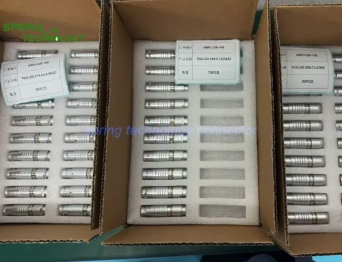


CBZC2BG Push-Pull Connector for Semiconductor Wafer Probers 2026: 2B Series 19-Pin 5 A PCB Socket for Wafer Test Equipment Interfaces for Canadian Client
The CBZC2BG-SFEM19-0000 is a CBZC2BG push-pull connector for semiconductor wafer probers — a 19-contact PCB-mounted connector with 19 low-voltage contacts, a compact 2B size, 90° PCB termination, metal shielding of 75 dB at 10 MHz and 40 dB at 1 GHz, and a durability of 5,000 mating cycles. Every specification in this guide is backed by the semiconductor test equipment interconnect engineering of Spring Technology.
Pain point: Interfacing a semiconductor wafer prober — where precision motion mechanisms, probe assemblies, sensor interfaces, vacuum systems and test interfaces all need low-voltage control and feedback lines inside one chassis, with signal integrity measured against nanometre-scale measurements?
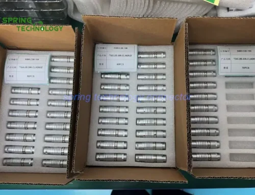
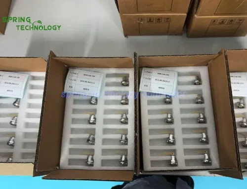
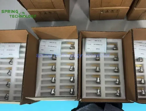
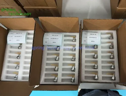
Core answer: For a Canadian client, Spring Technology supplied the CBZC2BG-SFEM19-0000, a 2B series fixed panel-mount socket serving as a CBZC2BG push-pull connector for semiconductor wafer probers. Wafer probers are used during wafer testing to precisely position probes onto chip test points and, together with testing instruments, perform electrical performance tests on the chips located on the wafer. Such equipment incorporates precision motion mechanisms, probe assemblies, control circuitry, sensors, vacuum systems and test interfaces, and its internal systems require numerous low-voltage control and feedback lines. This socket uses 19 low-voltage contacts with 90° PCB termination, rear-mounting capability and a push-pull self-locking mechanism; the 19-pin configuration uses 0.7 mm contacts with a maximum rated current of 5 A, suitable for wire gauges from 30 to 22 AWG.
1. Technical Parameters & Engineering Standards
This wafer prober socket is built on the ZCG.2B fixed socket platform (elbow PCB contact version), a mid-size circular connector family for professional industrial and test equipment.
- Latching Mechanism: Push-pull self-locking system (locks on insertion, releases quickly for removal)
- Recommended Hardware: Spring Technology Circular Connector
- Key Metric: 19 contacts × 0.7 mm; max. 5 A; 90° PCB contacts; 75 dB shielding at 10 MHz
| Parameter | Value |
|---|---|
| Socket (this order) | CBZC2BG-SFEM19-0000 — ZCG fixed socket, 2B shell, key G, 19 contacts |
| Contacts | 19 low-voltage contacts, 0.7 mm contact diameter |
| Rated current | Max. 5 A |
| Wire gauge | 30–22 AWG |
| Termination | 90° PCB elbow contacts, rear-panel mount design |
| Housing material | Chrome-plated brass metal housing, shielded structure |
| Shielding | Min. 75 dB at 10 MHz, 40 dB at 1 GHz |
| Mating life | 5,000 mating cycles |
| Shock resistance | 100 g |
| Vibration resistance | 15 g |
| Operating temperature | -45 °C ~ +125 °C |
| Application | Semiconductor wafer probers and probe station equipment |
2. Wafer Prober Connector Design Highlights
Wafer probing combines precision motion with dense low-voltage control. The design advantages below explain why this CBZC2BG push-pull connector for semiconductor wafer probers suits probe station equipment:
2.1 19-Pin Design for Multi-Channel Control and Feedback
- Wafer probers handle position control, motion feedback, sensor status monitoring and general equipment control simultaneously. The 19 low-voltage contacts with 0.7 mm diameter and a maximum rated current of 5 A let manufacturers assign contacts to control signals, feedback signals, auxiliary power or other low-voltage lines, reducing the need for multiple low-pin-count connectors inside the equipment.
2.2 90° PCB Configuration for Precision Equipment Layouts
- Probe testers house motion control boards, sensor interface boards and test control modules, so internal space and wiring layouts require precise design. The 90° PCB elbow contacts with rear-panel mount allow direct connection to the PCB, minimizing the space consumption associated with straight-style connectors and optimizing the interface between PCB and panel.
2.3 Push-Pull Locking for Equipment Maintenance
- Semiconductor testing equipment requires periodic calibration, maintenance and module replacement with frequent connection and disconnection of interfaces. The push-pull self-locking system locks automatically upon insertion and releases quickly for removal without repetitive threaded rotation, well suited to module maintenance and rapid interface operations, with a mating cycle life of 5,000 operations.
2.4 19-Pin High-Density Connection Reduces Interface Count
- Wafer probers connect to multiple sensors and control modules, and using a separate connector for each signal type would increase the number of interfaces on the PCB and panel. Integrating 19 low-voltage contacts within a Size 2B housing consolidates related low-voltage lines into one connector, reducing connector count and simplifying internal wiring harness layouts.
2.5 Metal Shielding for Semiconductor Test EMC
- Semiconductor test equipment contains numerous precision electronic circuits alongside high-speed digital control and motion control systems, making EMC critical. The chrome-plated brass metal housing and shielded structure deliver minimum shielding performance of 75 dB at 10 MHz and 40 dB at 1 GHz, aiding overall EMC design for equipment demanding high signal integrity.
2.6 5 A Rated Current for Control and Auxiliary Power
- With a rated current of 5 A across 19 low-voltage contacts, specific contacts can be assigned to control lines, sensor lines or low-voltage auxiliary power supplies depending on the circuit design, letting a single connector handle multiple low-voltage functions and increasing the integration level of the equipment interface.
2.7 5,000-Cycle Mating Durability
- Semiconductor test equipment runs long-term and undergoes repeated mating during installation, commissioning, maintenance and module replacement. A rated service life of 5,000 mating cycles meets the demands of professional test equipment and helps reduce maintenance costs from frequent connector replacement.
2.8 Shock, Vibration and Temperature Resistance
- Wafer probers incorporate precision motion mechanisms that require stable mechanical connections. With 100 g shock tolerance, 15 g vibration performance and an operating temperature range of -45 °C to +125 °C, the connector provides a reliable connection foundation for long-term semiconductor test operation.
3. 2B Series Connector Family Overview
The 2B shell is part of Spring Technology’s push-pull self-locking connector family, used in semiconductor test, precision measurement, industrial and professional equipment. The same platform serves this wafer prober socket and scales across pin counts and contact variants.
3.1 Available Configurations
- Sockets: ZCG.2B fixed sockets, including the elbow (90°) PCB contact version in this order.
- Pin counts: 2 to 26 contacts across the 2B shell, including the 19-pin high-density layout.
- Termination: 90° right-angle PCB contacts, straight PCB contacts and solder versions.
- Materials: chrome-plated brass shells with shielded structures across the platform.
3.2 Customization Services
- Custom contact allocations and part numbers (such as the CBZC2BG-SFEM19-0000) matched to each system’s control and feedback plan.
- Panel hole and PCB footprint customization for prober layouts.
- Shielding and EMC verification for precision measurement circuits.
- Pre-wired motion control and sensor harnesses.
4. Applications: Semiconductor Wafer Probers
Wafer test cells need interfaces that stay electrically quiet and mechanically stable. This CBZC2BG push-pull connector for semiconductor wafer probers serves the prober’s internal modules.
4.1 Control Modules
Prober control modules connect through the 19-pin interface, with contacts assigned to control signals, feedback signals and auxiliary power.
4.2 Sensor and Motion Control Interfaces
Sensor interfaces and motion control units link to the main board through the same connector family, keeping harness layouts compact.
4.3 Probe Station Equipment
Probe stations that position probes onto chip test points benefit from the shielded, high-density interface and its maintenance-friendly locking.
5. Frequently Asked Questions (FAQ)
Conclusion & Call to Action
This 2B connector delivery for the Canadian client shows how Spring Technology serves semiconductor test equipment — from the 19 contacts and 90° PCB termination of the CBZC2BG-SFEM19-0000 to its shielding and maintenance-friendly locking, every detail was aligned with the customer’s wafer prober requirements. Spring Technology also provides professional customization services for both push-pull connectors and cable assemblies, offering tailored solutions to meet your specific technical requirements.
For more information about our 2B series connectors or to discuss your requirements, contact us at [email protected] or [email protected], or visit our website.
Building a wafer prober or probe station? Send us your control and feedback requirements — our engineering team will respond with a tailored CBZC2BG push-pull connector proposal for your semiconductor wafer probers within 24 hours.
Further Reading
- Push-Pull Connector for Automated Test Equipment 2026: CBZC1BG-SFSM07-0000 and CBTA1BG-SMSM07-0000 for High-Precision Test, Measurement and Industrial Robotics for US Customers
- CBTG2FN Push-Pull Connector for Precision Machine Tools 2026: CBTG2FN-SMSM09-D520 and CBZL2FN-SFPM09-S000 for Multi-Channel Miniature Sensor Aggregation for Russian Client
- CBTG31FN Push-Pull Connector for Machine Vision Cameras 2026: 31F Series 19-Pin Connector for Industrial Vision and AOI Systems for US Market
- CBZC2BG Push-Pull Connector for Portable Spectrum Analyzers 2026: 2B Series 4-Contact 90° PCB Socket for RF Test Instrument Interfaces for Canadian Client
- Push-Pull Connector for Data Acquisition 2026: CBZG0BG-SFSM06, CBZG1BG-SFSM06 and CBZG0BB-SFSM06 for Test, Measurement and Industrial Data Acquisition for Russian Customers
- ZCG.2B Fixed Socket With Elbow (90°) Contact — Product Page
- 2B Series Connector